Because of the increasing demand for electronic performance nowadays, electronic components are becoming miniaturization, small, and high-integrity. As the spacing between adjacent conductors shrinking, residues or other contaminants on printed circuit boards (PCBs) draws more and more attention by people. While traditional surface mount technology (SMT) makes good use of low-residue and no-clean soldering processes, in high-reliability products, structural densification of products and miniaturized assembly of components make it increasingly difficult to achieve suitable size. Cleaning levels due to increased product failures due to cleaning issues.
Influence of contaminant residues on PCB spot welding
1. Electrochemical Migration
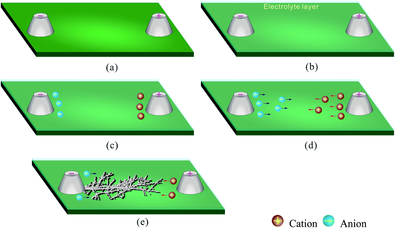
Electrochemical migration, or ECM, is the movement of ions through particular media under the influence of an electromagnetic field, such as magnetic flux. Some ionic impurities, such as activators and salts in flux residues, can become electrolytes in PCB products when the ambient humidity changes, causing changes in spot welding properties.

When these kinds of PCBs work, shorts can occur between spot welds under stress voltage,, causing intermittent failures and reducing the reliability of the PCBs. The process consists of three steps: path formation, initialization, and dendrite generation. The path formed begins with the dissolution of metal ions in the electrolyte, a weak acid formed from the combination of chlorine and bromine residues in the flux and water in the air. When metals dissolve in weak acids, filaments are created. Therefore, elements including ion surplus, voltage bias and humidity must be required to achieve the mechanism of electrochemical effectiveness. In addition, electrochemical effects are also affected by temperature, humidity, product, conductor material, conductor spacing, type and amount of contaminants.
2. Creep corrosion
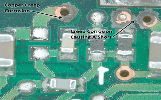
The formation of copper or silver sulfide crystals on the surface of the PCB is known as creep corrosion. Different from electrochemical migration, the existence of contamination sources and moisture in the environment can promote creep corrosion without the necessity for a voltage differential. When sulfur in the air combines with copper or silver on the PCB, copper or silver sulfide is produced. These chemical compounds like copper sulfide and silver sulfide will grow in any direction, opening or shorting the thin wires between the pitch leads, which will eventually lead to poor quality PCBs. The risk of this corrosion will certainly increase as PCB size gets smaller and components are miniaturized. Creep corrosion is particularly frequent in industrial control electronics and airplanes due to the presence of more contaminating gases in the surrounding air. Another reason is the surface finish - HASL with lead, which means the outer copper foil of PCB will be protected by tin-lead. Some copper or silver will be exposed to air if the moisture capacity of the soldering process is not at the standard level. The risk of creep corrosion will be greatly increased when the environment is deteriorated by the influence of moisture.

3. Tin Whisker
Tin whiskers are a major concern for professionals. Through extensive studies based on the chemical and physical parameters of tin whisker generation, experts pointed out that tin alloys proliferate with other metals under the action of high temperature and high humidity, which will contribute to the formation of intermetallic compounds (IMCs). In this situation, as the voltage stress in the tin layer rises rapidly, tin ions migrate along grain boundaries to generate tin whiskers, increasing the chance of a short circuit. So during reflow, when the tin alloy becomes solid, some of the halides and bromides in the flux flowing from the solder paste act as ionic contaminants, resulting in the formation of tin whiskers. In addition, tin whiskers are often affected by the degree of ionic contamination, and it can be concluded that the higher the degree of ionic contamination, the higher the density of tin whiskers.
![]()
Some questions about cleaning PCBs
1. Pollutants
The objects that need to be cleaned after soldering are mainly the residues left on the PCB. Based on their chemical properties, residues can be divided into three categories: water-soluble polar residues, water-insoluble non-polar residues, and water-soluble but non-polar residues that cannot be converted into ionic organic compounds. These contaminants are believed to be the key causes of changes in PCB performance or even failure. Therefore, it is very necessary to completely clean the residue. In addition, PCBs are moving towards high density and fine pitch, and PCB cleaning becomes especially important.
2. Flux
Flux residues are the most important part of PCB manufacturing, which is why flux residues must come first in cleaning processes. J-STD-004 divides fluxes into four types based on chemical properties: rosin, resin, organic, and inorganic, with each category further subdivided depending on flux/flux residue activity level and halide weight. This is also due to the fact that all fluxes have the ability to dissolve oxides and accelerate solder infiltration. In the PCB manufacturing process, flux is used for wave soldering, reflow soldering and hand soldering, and it is best to choose only one type of flux. For the cleaning of the entire PCB, it is just the process of removing one kind of flux.Due to the complex nature of these fluxes leading to the complexity of their combination, cleaning can be challenging if picking up several different types of flux.
3. Cleaning process
Three types of cleaning tools are commonly used in PCB cleaning: solvent cleaning, semi-aqueous cleaning and water cleaning. Solvent cleaning refers to the process of cleaning PCBs using solvent-based media. In this process, drying takes place in a separate facility. Semi-aqueous cleaning involves solvent cleaning of PCBs followed by water removal of organic solvents from the PCBA to eliminate flux and other impurities. Water cleaning refers to the process of cleaning a PCB with only water. A proper cleaning technique should be implemented based on the features of the equipment and goods in order to considerably increase the PCB's dependability.
4. Cleaning solvent
Depending on the type of flux, a cleaning solvent that matches the type of flux should be selected. There are different types of cleaning solvents and cleaning solvent components. According to the regulations of the Japan Industrial Cleaning Council (JICC), cleaning solvents are classified according to the rinsing process. Cleaning solvents are split into two categories: water-soluble and non-water-soluble cleaning solvents. Cleaning solvents that are water-soluble require water during the washing process, whereas cleaning solvents that are water-insoluble do not.
5. Cleaning equipment and cleaning methods
At present, the cleaning equipment is mainly divided into intermittent type and honeycomb type. The cleaning methods include ultrasonic, spray, immersion, jet, bubble and so on. Cleaning methods for common cleaning equipment include spraying or gas phase cleaning, as well as mechanical cleaning methods such as stirring, rotating, and so on.

6. Cleaning standard
Different cleaning objects have different cleaning standards. Every products have various usage settings, shelf time, and technical specifications, as a result, appropriate cleaning standards must be consistent with the relevant industry and product features. According to IPC standards, the general highest cleaning levels are: No ionic contaminants; or flux residue; or insulation resistance.
Conclusion
Overall, the risk of physical and chemical failure will be greatly reduced, thereby improving the PCB's reliability, as long as the negative effects of residues related to the failure mechanism of PCB spot welding are fully understood, and appropriate cleaning solvents and methods are selected according to the cleaning process design.
If you are looking for a PCB manufacturer, PCBGOGO is fully compliant with the ISO 9001:2015 quality management system and UL certification. Reliable and affordable PCB services can save your time and money on your way to success.
- Comments(2)
W****rry
May 31.2024, 18:03:35
D****ien
Jan 05.2024, 16:15:04

