Every electronic device we use today is susceptible to electromagnetic interference (EMI). A printed circuit board (PCB), integrated chips, interconnect, and I/O cables comprise an electronic system. At high frequencies, the interconnects tend to act as antennas, resulting in EMI, depending on the length of the interconnects and the current carried by the conductors. These EMI radiations interfere with other devices in the area. International standards exist to limit the level of emissions. As a result, measuring and controlling electromagnetic radiation is critical.
Various strategies can be used to reduce electromagnetic interference (EMI) on a PCB board. The various aspects must be considered and handled properly.
1. Grounding
2. Separation
3. Shielding
Separation
A trace is any path that carries electricity from the driver to the receiver. These traces can create an antenna when they bend or cross, which can result in EMI. It is advised to separate all signals from other traces because of this. It assists in minimizing crosstalk (prevent unwanted transfer of signals between the systems).
It is important to separate AC and DC systems on the PCB, separating AC and DC systems, including their chips and traces, will help prevent unwanted transfer of signals between the systems. You can cut gaps in the ground plane between the components that need to be separated if there isn't enough room on the board to physically separate AC and DC systems. Using gaps in the ground plane to your advantage will help you reroute currents around delicate systems. Gaps in the ground plane will cause any currents running through the plane to go around the gaps.
1. Separating Power rails: There should be separate power rails for AC and DC components in every AC/DC PCB. A voltage transient can be produced by DC components by drawing spikes from their power source. While your AC components might (or might not) be able to function in the presence of this voltage transient, they won't function to their fullest potential. The circuit may malfunction completely or exhibit problems in its AC components if the voltage transients are too large. This is why it is important to have separate power rails to keeps AC components away from DC components
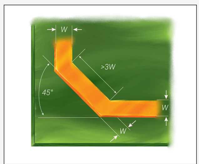
2. Avoid right angles and take a 45° turn instead: When a trace comes into contact with a 90° curve, the capacitance rises, changing the characteristic impedance value and causing reflections. By substituting 45° turns for acute bends, it can be prevented.

3. Careful use of Vias: Vias are utilized on multi-layer PCBs for signal routing, so use them like an expert. A good designer must be aware of the capacitance and inductance effects that each via has. Therefore, essential traces should be routed on the same layer and vias should be avoided wherever possible. Reflections are caused by an impedance mismatch between the via and the trace, which is caused by the parasitic capacitance and inductance in the vias. When vias are unavoidable, care should be taken to position the ground vias close to the signal vias. By referencing the signals to linked grounds, this prevents changes in the characteristic impedance value and, consequently, reflections. The same number of vias should be placed in both traces of differential pairs where vias cannot be avoided. It is also critical to account for any signal delay caused by a via. This can be accomplished by using the same number of vias in both legs of the differential pair or by incorporating serpentine routing on the leg lacking a via.
4. Careful use of traces: As you may be aware, high-speed PCBs frequently suffer from EMI issues. Long traces that form transmitting or receiving antennas can pose an EMI risk. Longer traces also cover more distance, increasing the likelihood that sensitive circuits will be affected along the way. Using short, direct-path traces will help reduce EMI risk from both antennas and trace proximity. No one intentionally routes a trace so that it acts as an EMI antenna, perhaps a high frequency changed the impedance of a capacitor, or a return current caused an unexpected loop in the ground plane. Whatever the reason, shortening traces is the best way to reduce antenna radiation. Because antennas can transmit and receive, traces in both "noisy" and "quiet" circuits should be cut. A smaller antenna will always emit or receive less signal than a larger one. Traces aren't the only things on the PCB that can emit EMI. When a trace crosses through a gap in the ground plane, it acts as an antenna. Keep traces short and direct, but not at the expense of crossing ground plane gaps. It is important to note that when routing a differential pair, make every effort to keep their traces parallel. Parallelizing a differential pair helps cancel out any radiated EMI and aids in trace length matching.
Grounding
The ground plane delivers the lowest inductance value when the signal returns to the source from the load, hence use the entire ground plane. Even though a ground needs its own PCB layer, a two-layer PCB may not always allow for this. In these cases, designers utilize ground grids, where each grid's inductance is dependent on the spacing between them. There should be the same number of vias in both traces.
In some mixed-signal designs, an effort is made to keep analogue and digital circuitry apart in order to prevent electromagnetic interference (EMI). However, having two completely independent grounding planes could result in different references for some circuit components. Your circuit may have faults as a result. A ferrite bead and Schottky diodes can be used to connect different ground planes in circuits using a single data converter. However, the two grounding planes can be combined for more universal systems, or only one plane can be used. This is provided that the return paths of the AC and DC currents do not intersect, as this would result in "crosstalk." It is strongly advised to use a single, sturdy ground plane, preferably with well-considered current return pathways.
A star ground can be a great solution when designing a PCB with only one mixed-signal IC. Instead of an entire plane, the star ground makes use of a single point as a reference. For converters and some other mixed-signal chips, the manufacturer usually recommends connecting the AGND and DGND pins outside of the chip; this connection can serve as your star ground. You can also connect the two ground planes at that point if you're using two separate ground planes with a single mixed-signal IC. One complication with star grounds is that the connections to the star ground must be as long as possible.
Mixed-signal system grounds necessitate careful distribution planning because return paths must be checked to reduce EMI and "crosstalk." When everything looks the same, distribution planning becomes extremely difficult. I recommend that you colour code your components and nets in your PCB design software so that you can visually separate AC and DC systems, or pins if you're working with mixed-signal ICs.
Shielding
Some components, particularly small, high-speed parts, will generate EMI regardless of design rules. Fortunately, shielding and filtering can reduce the effects of EMI. Shields are especially useful for isolating components from EMI that may occur elsewhere on the PCB. They are most commonly used over RF outputs, as well as inputs and amplifier stages, because these are the sections of a circuit that are most likely to be affected by/cause EMI. To isolate the RF module and amplifier from other noise in the circuit, it is important to use a shield.
Enclosure: Physical shields are metallic packages that encase an entire board or a portion of it. Their goal is to prevent EMI from entering the board's circuitry, though the specific methods vary depending on the source of the EMI. Component shields can be used to encase a specific component that produces EMI, allowing it to connect to ground, reducing the antenna loop size, and absorbing EMI. To protect against EMI from outside sources, other shields may encase the entire board. Typically, these devices are made of metal or conductive foam.
Cables: Cables that carry analogue and digital currents generate the most EMI problems. They cause these problems by generating parasitic capacitance and inductance, which is especially problematic for high-frequency signals. Fortunately, shielding these cables and connecting them to ground at both ends helps to cancel out EMI interference.
- Comments(12)
**
Jun 20.2024, 12:52:40
p****nda
May 06.2024, 16:32:37
r****lla
Apr 11.2024, 12:17:13
J****rse
Feb 13.2024, 10:51:59
I'm thankful I stumbled upon the killer papers review. before deciding to utilize their services. This review opened my eyes to their inadequacies in delivering effective academic support. It saved me not only time but also the potential frustration of engaging with a service that might not meet my academic needs. The insights from the review guided me towards making a more informed decision about where to seek help, ensuring that I choose services that genuinely offer value and reliable assistance for my studies. This experience underscored the importance of thorough research and reading reviews before committing to any academic assistance platform.
https://translate.google.com/
p****nda
Feb 02.2024, 12:17:43
C****den
Jan 26.2024, 01:04:32
C****den
Jan 26.2024, 01:04:21
<a href="https://writemyessaysos.com/"> essay writer online </a>
[This link will be renamed](http://www.edmodo.com)
**
Jan 05.2024, 21:16:38
****low
Dec 27.2023, 19:02:17
<a href="https://google.com/">google</a>
[URL=https://google.com/]google[/URL]
"google":https://google.com/
[google](https://google.com/)
****low
Dec 27.2023, 19:01:48
**
Dec 21.2023, 07:05:41
I appreciate the practical tips you always include in your posts. Family announcement
