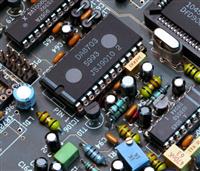
Printed Circuit Board (PCB) assembly is a critical stage in electronics manufacturing, where various components are soldered onto a circuit board to create functional electronic devices. As technology advances, the landscape of PCB assembly evolves, incorporating new methodologies and technologies.
Here, we delve into the key factors to consider in PCB assembly, including emerging technologies and methods utilized by leading manufacturers like PCBGOGO.
Component Selection:
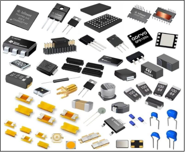
The selection of components plays a pivotal role in PCB assembly process. Manufacturers must consider factors such as component compatibility, availability, reliability, and cost-effectiveness. With advancements in miniaturization, surface-mount technology (SMT) components have gained prominence over through-hole components due to their smaller size, higher component density, and improved performance.
PCB Design and Layout:
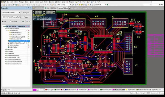
A well-designed PCB layout is crucial for efficient assembly and optimal performance of electronic devices. Factors such as signal integrity, thermal management, and manufacturability should be carefully considered during the design phase. Advanced design tools and techniques, including computer-aided design (CAD) software and simulation tools, aid in optimizing PCB layouts for improved functionality and manufacturability.
Assembly Process:
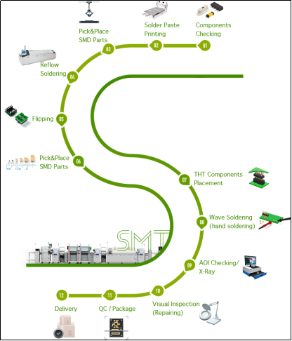
The assembly process encompasses various stages, including:
· Solder paste application
· Component placement
· Soldering, inspection
· Testing.
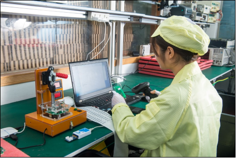
Advanced assembly techniques such as automated pick-and-place machines, reflow soldering, and selective soldering are employed to enhance efficiency, accuracy, and consistency in the assembly process. The adoption of lead-free soldering processes aligns with environmental regulations and promotes sustainability.
Quality Assurance and Testing:
Quality assurance measures are essential to ensure the reliability and functionality of assembled PCBs. Inspection techniques such as automated optical inspection (AOI) and X-ray inspection help identify defects such as solder joint defects, component misalignment, and shorts. Functional testing, including in-circuit testing (ICT) and automated testing, verifies the performance of electronic devices before they are deployed in the field.
Advanced Technologies in PCB Assembly:
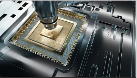
Leading manufacturers like PCBGOGO leverage advanced technologies to enhance the efficiency and quality of PCB assembly. This includes the integration of artificial intelligence (AI) and machine learning algorithms for process optimization, predictive maintenance, and defect detection. The adoption of additive manufacturing techniques such as 3D printing for rapid prototyping and customized PCB production offers flexibility and cost-effectiveness.
Supply Chain Management:
Effective supply chain management is essential to ensure the availability of components and materials required for PCB assembly. Collaborative partnerships with component suppliers, inventory management systems, and just-in-time (JIT) manufacturing practices streamline the supply chain, minimize lead times, and reduce production costs.
Environmental Sustainability:
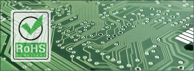
With growing concerns about environmental sustainability, manufacturers are increasingly focusing on eco-friendly practices in PCB assembly. This includes the use of recyclable materials, energy-efficient manufacturing processes, and waste reduction initiatives. Additionally, the implementation of green manufacturing standards such as RoHS (Restriction of Hazardous Substances) compliance ensures the safety and sustainability of electronic products.
Steps in PCB Assembly:
1. Stencil Printing:
Solder paste, a mixture of tiny solder particles and flux, is applied onto the bare PCB through a stencil. This paste is deposited onto the pads where components will be soldered.
2. Component Placement:
Automated machines or manual labor place surface-mount components onto the solder paste on the PCB. This step requires precision to ensure accurate placement of each component.
3. Reflow Soldering:
The PCB with components is passed through a reflow oven where it undergoes controlled heating. The solder paste melts, creating a permanent bond between the components and the PCB pads.
4. Inspection:
Automated optical inspection (AOI) and X-ray inspection are performed to detect any defects such as misaligned components, solder bridges, or missing components. This ensures the quality and reliability of the assembled PCB.
5. Through-Hole Component Insertion:
If through-hole components are used, they are inserted into pre-drilled holes on the PCB manually or with automated insertion equipment.
6. Wave Soldering:
The PCB with through-hole components is passed over a wave of molten solder, which flows through the holes and creates solder joints between the components and the PCB.
7. Secondary Inspection:
After wave soldering, another round of inspection is conducted to verify the quality of solder joints and overall assembly integrity.
8. Cleaning:
Flux residues and other contaminants are removed from the assembled PCB using cleaning agents and equipment. This ensures the cleanliness and reliability of the final product
9. Testing:
Functional testing, in-circuit testing (ICT), and/or automated testing are performed to verify the functionality and performance of the assembled PCB. This step ensures that the PCB meets the required specifications and standards.
10. Packaging and Shipping:
Once the PCB assembly passes all quality checks, it is packaged according to customer requirements and shipped to its destination for further integration into electronic products or systems.
Key Factors in Quality PCB Design:
· Separate analogue and digital grounds to prevent noisy signals and abnormal functioning, manually routing grounds to avoid auto-routing mishaps.
· Place capacitors between input power and ground for each digital IC.
· Keep high frequency tracks short and ensure signals with high frequency have a ground plane below them, avoiding gaps.
· Maintain separation between analogue and digital circuits.
· Keep analogue ground and digital grounds separated but connected to a common point.
· Avoid 90 degree bends in tracks, opt for 45 degree bends to minimize noise and signal reflections.
· Prioritize wide power and ground tracks to accommodate higher current limits, placing them first in the design.
· Minimize the use of auto-routing and manually route when possible.
· Ensure no unconnected copper fills on the PCB, either ground them for heat dissipation or remove them.
· Avoid placing vias under components; use through-hole components as vias if necessary.
· Keep drill size for holes and vias to a minimum to optimize PCB space and manufacturing efficiency.
In conclusion, printed circuit board assembly is a complex process that requires careful consideration of various factors to ensure the production of high-quality electronic devices. By embracing emerging technologies, advanced assembly methods, and sustainable practices, manufacturers can enhance efficiency, reliability, and environmental responsibility in PCB assembly. Companies like PCBGOGO exemplify the integration of innovation and expertise to deliver superior PCB assembly solutions in today's dynamic electronics industry
- Comments(13)
T****ben
May 09.2024, 15:36:10
**
Apr 16.2024, 15:48:01
p****nda
Mar 18.2024, 17:12:20
M****SEO
Mar 12.2024, 19:50:18
| ????? | https://www.mt-on.com/ |
M****SEO
Mar 12.2024, 18:28:33
M****SEO
Mar 11.2024, 21:04:56
| ????? | https://www.mtpolicee.com/ |
**
Mar 11.2024, 19:24:12
**
Mar 11.2024, 14:45:52
J****erv
Mar 06.2024, 22:41:27
Quora offers valuable insights into the best essay writing services. By checking the community's recommendations, you can find reliable assistance for your academic needs. Don't miss out on this resourceful platform when searching for top-notch writing services. Trust the https://www.quora.com/Can-I-trust-a-lab-report-writer/ community to guide you in the right direction!
n****eta
Mar 02.2024, 02:10:52
M****ali
Feb 22.2024, 17:35:49
R****son
Feb 22.2024, 12:05:20

