The PCBs are the physical support of electronic components and the carrier for their electrical interconnection. They have been used widely in Medical Devices, Consumer Electronics, Industrial Equipment due to their high reliability, high density, and other unique characteristics. For many years, the demand for PCBs has shown rapid growth in terms of output and performance, which leads to a higher requirement for PCB & PCBA quality control.
Regardless of the application, all PCBs must function correctly according to the project specifications. Thus, PCB & PCBA testing is an essential part of the manufacturing stage to find out any possible defects or faculty that could cause the board to malfunction. In this article, we will discuss some common PCB & PCBA testing techniques operated inside the factories of PCBgogo, a professional PCB & PCBA manufacturer in China.
1. Benefits of the PCB & PCBA testing
PCB & PCBA testing allows us to identify and solve the critical errors of the boards at an earlier stage. It helps to reduce cost, save time and optimize safety. If the defective boards are not screened out in time and allowed to flow into the final production process, it will inevitably lead to more waste. Fixing defects on a finished product is more difficult and costly. In the production process of electronic products, the cost loss caused by defects has different degrees in each stage. The earlier the defects are found, the lower the cost of modifications.
2. Defects to be tested on PCB and PCBA
Following are the common defects for the PCB and PCB Assembly to be tested during the manufacturing process.
2.1 For PCB
Open
Insufficient
Short
Missing electrical component
Misaligned
Defective electrical component
Wrong component
Excess solder
Missing non-electrical component
Wrong orientation
Defective non-electrical component
2.2 For PCBA
2.2.1 Soldering defects
Open circuits
Solder bridges
Solder shorts
Insufficient solder
Solder void
Excess solder
Solder quality
2.2.2 Component defects
Lifted lead
Missing component
Misaligned/misplaced components
Incorrect component value
Faulty component
2.2.3 BGA and CSP defects
BGA shorts
BGA open circuit connections
3. Common PCB& PCBA testing techniques
3.1 Manual visual inspection
Manual visual inspection is the most traditional inspection technique that uses a magnifier or a calibrated microscope to check whether the assembled board is qualified through the operator's visual inspection. It is sufficient to find out the solder faculty and other visible defects when the circuit boards are relatively simple with few components and soldering connections.
This technique is low-cost without requiring a test fixture. However, it is subject to human error. Some defects might be missed if the inspectors get bored or tired when performing such repetitive tasks. It also has the disadvantages of high long-term cost, inconsistent detection, and difficulty in data collection. With the increasing PCB yield, the denser PCB designs, and smaller components, this testing technique becomes infeasible.
3.2 Automated optical inspection(AOI)
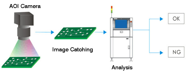
Automated optical inspection (AOI) is a widely accepted testing technique for both PCBs and PCB assembly. It uses high-resolution cameras that automatically scan the circuit boards. By comparing the images captured and the original design files, potential defects can be found at an early stage.
AOI has usually performed ahead of and after the solder reflow stage. The faculty boards found will be reworked. The cost of fixing the defects at this time is almost 10 times lower than that after the final test. To achieve a high-quality standard, some PCB manufacturers like PCBgogo will carry out AOI multiple times during different production processes.
3.3 Automatic X-ray inspection(AXI)
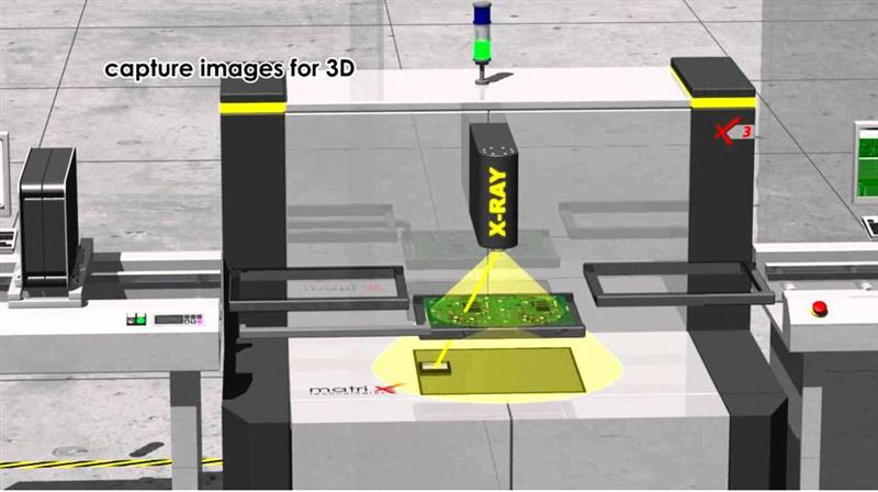
Although AOI can inspect many types of defects (component placement, solder shorts, missing solder, etc.), it faces difficulty in detecting the connections and solders hidden underneath the package especially for the BGA package. Automatic X-ray inspection was then developed. Based on different absorption of X-rays when passing through the object, it can reveal the structure of the objects hidden from view.
AXI is mainly used to detect defects in ultra-fine pitch and ultra-high-density circuit boards, including bridges, missing chips, poor alignment, and other defects generated during the assembly process. For BGA and solder balls, AXI is the only alternative to test the soldering quality. As the trending of surface mount technology (SMT) brings smaller components and new chip packages as well as the increased complexity of double-sided and even multilayer boards, applications for automated x-ray inspection are constantly growing. In PCBgogo, AXI is available when you ordering PCB assembly services.
3.4 Bed of nails testing
A bed of nails tester is a traditional electronic test fixture performed after the PCB assembly process. It has an array of small, spring-loaded pogo pins aligned using tooling pins to make contact with test points on a circuit board and are also connected to a measuring unit by wires. This technique indicates whether the assembly is correctly fabricated by checking shorts, opens, resistance, capacitance, and other fundamental variables.
The whole testing process is software controlled, taking a few seconds to tens of seconds to test a single board. As the contact is made directly on the test points within the circuitry of the DUT, it can correctly test individual components and measure their performance. However, requiring a specific fixture for each type of PCB makes it costly for PCB prototype testing. In the case of small-batch PCB orders, it is a favorable option.
3.5 Flying probe testing
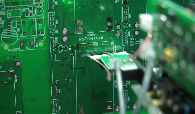
The flying probe tester is an improvement over the bed of nails tester. It does not require a fixture, saving the cost of processing specific probes and manufacturing the custom tools. With 2 or more movable probes instead of a closely arranged bed of nails, it can detect PCBs with high component density and small pitch widths.
Flying probe testing is commonly used for the test of analog components, analog signature analysis, and short/open circuits. It becomes an alternative to the bed-of-nails technique for contacting the components on the PCBs. However, while flying probe testing has lower initial costs, its test speed is much slower than the bed of nails tester. This quality makes it an ideal testing technique for PCB prototypes and small-batch orders but less effective for large-scale production. In PCBgogo, all the boards will undergo flying probe testing before being delivered to the customers.
Image courtesy:pcbgogo.com
3.6 Functional testing
Functional testing, as the name suggests, tests whether the assembled PCBs will function exactly as intended. The tester simulates the PCB’s final electrical environment to verify that the equipment will power up. It usually performs in the last step of the manufacturing process. Although it is complex and costly regarding the testing program, it provides great quality assurance.
4. Conclusions
PCB & PCBA testing is a necessary part of manufacturing. It can find out the defects at an earlier stage, help save money and prevent issues before reaching the final production phase. With the miniaturization of components and increasing complexity of PCB design, there is a higher need for more advanced testing techniques. However, decisions about what tests to request should be made according to the quality requirement of the boards. Although an appropriate combination of all the testing techniques can identify almost all the defects, it is critical to consider the most cost-effective solution for your specific needs.
PCBgogo processes all the testing equipment described above and is staffed with experienced engineers and technicians working for your PCB and PCBA orders.They can provide expert support and be your trusted partner for your next PCB projects.
- Comments(7)
E****ith
Jun 19.2024, 14:41:26
**
Apr 10.2024, 19:00:00
**
Apr 08.2024, 21:18:10
**
Apr 04.2024, 21:28:07
**
Mar 12.2024, 18:27:39
**
Mar 11.2024, 15:40:50
J****phy
Feb 03.2024, 10:18:56


