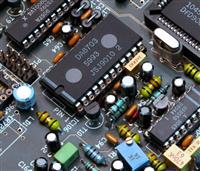
PCB panelization is to combine multiple separate circuit boards that share the same number of layers, thickness, and other parameters into one large board. In this way, a variety of boards can be produced at one time which speeds up the production and lowers the cost of PCB prototypes.
Benefits of PCB panelization
Improve the utilization rate of the board
Generally, the copper-clad laminates used in PCB production are of fixed size. Rotating specially shaped boards from 90° to 180° and fitting them into the standard size panel can maximize space and reduce waste.
Figure 1 PCB rotating in a panel
Facilitate SMT assembly process
It is more effective to process multiple boards at once. Several boards into a panel increase the number of components for the placement, which also improves the efficiency of the Pick and Place machine.
Types of PCB panelization
V-cut
V-cut is the most popular panel method for PCB manufacturing. It refers to a dividing line cut by a rotary cutter at a specific position of the connected board that is used to de-panel the board after the PCB assembly is completed. Because the cut shape looks like the letter V, it is called V-cut. The connection of the board in this place is relatively thin and thus it is easy to break the board.
Figure 2 PCB with V-cut
Tab-routing
As the separation line of V-cut can only be straight, V-cut is only suitable for the panel connection of regular PCB boards, such as PCBs with a square or rectangular shape. For specially-shaped PCB boards such as circular ones, Tab-routing is used instead. Tab-routing is to connect two boards with several stamp holes at the edge, which is easy to break. Tab-routing fits any shape of PCBs but it is rather complex and expensive.
After separation, additional material such as burrs might be left at the edge, which sometimes causes troubles in the assembly process.
Figure 3 PCB with Tab-routing
Methods of PCB depanelization
V-cut scoring machine
In PCB factories, a scoring machine is used to cut the board along the location of the V-Cut line. The height of the blade can be adjusted up or down to match the thickness of different V-Cut requirements. Although it is the simplest to break the boards, this V-cut method has some drawbacks. First of all, it can only cut a single straight line and cannot change the direction. This is because the scoring machine uses a chainsaw with two upper and lower discs so it only fits boards with straight edges. Secondly, V-Cut is not suitable for PCBs with thicknesses less than1.0 mm as the V-cut groove will destroy the structural strength of the board. When there are relatively heavy parts placed on the board with a V-Cut design, the board will become easy to bend under the effect of gravity, which may lead to non-wetting or shorts in the SMT assembly process.
Router
The router is ideal for PCB requiring high reliability and quality assurance. This technique produces no straining so it is less likely to cause crake on the components or solder joints due to bending force. Technically, it can solve most of the problems that a V-cut design may occur but it is much more expensive and complex.
Hand break
The hand break is to break the board along the V-cut or Tab route using a proper fixture. Some engineers might break the board manually. However, it is not recommended to do so as the bending of the board might lead to cracks in the components, especially capacitors and BGA parts, thereby reducing the yield and reliability of final products.
Some key terms
Breakaway
The breakaway is an additional space on both edges of the PCB board, normally 5mm wide without any SMD components placed on it. The current SMT production line is highly automated, and the PCB board flows to different assembly procedures automatically by conveyor belts, which may damage the electronic parts around it. The breakaway allows PCB to move smoothly through the SMT lines. It only serves to facilitate the production and would be removed after the production.
Fiducial mark
Fiducial marks are designed for the automatic machines to align themselves during the assembly process. The machine identifies the fiducial marks on the PCB and uses image recognition so they can locate the exact placement of each component. Fiducial marks affect the accuracy of component placement. They are crucial to SMT assembly.

Figure 4 Fiducial mark on a PCB
Conclusion
PCB penalization is conducted to maximize the panel space and improve the efficiency of the SMT assembly process. Considering the design, cost, and other factors, V-cut or Tab route is designed for depanelizeing the final boards. In order to receive high-quality panelized PCBs, you should work with an experienced PCB manufacturer like PCBGOGO that has good knowledge of those panel guidelines.
- Comments(14)
**
Jun 27.2024, 21:12:24
**
Jun 27.2024, 21:11:13
**
Jun 27.2024, 21:10:59
**
Jun 27.2024, 21:10:49
**
Jun 27.2024, 21:09:36
**
Jun 23.2024, 23:01:36
http://truediamond.co.uk/
**
Jun 15.2024, 17:57:42
E****ina
Jun 04.2024, 11:34:58
d****ter
Jun 02.2024, 01:07:36
**
Apr 24.2024, 21:36:55
PCB panelization is the process of combining multiple individual printed circuit boards (PCBs) into a single larger panel. When students pay for assignment, they miss out on valuable learning opportunities and fail to develop essential skills, such as critical thinking, research, and writing. Moreover, submitting work that isn't their own violates academic integrity policies and may lead to severe consequences, including academic penalties and reputational damage.
m****lam
Apr 07.2024, 17:28:36
m****lam
Apr 03.2024, 17:56:15
s****sss
Mar 17.2024, 17:03:31
P****yly
Jan 30.2024, 17:47:54


